There are a couple of ways to control WS2812B and its clones. Among them, the method that uses SPI bus via DMA would be the easiest choice for the following reasons; Firstly SPI bus is ubiquitous. Secondly DMA minimizes the burden of the processor and handles timing with hardware. No code is involved in transferring data. Thus once proper SPI clock is chosen, operation is quite reliable as well. Only downside is that you have to dedicate one SPI port for the control of the LED, since you cannot share this line with any other SPI devices
The timing of SK6812 is shown below. There are slight variations in the actual timing between devices. But basically all use the same high/low ratio, namely 1:3 for logic zero and 2:2 for logic one.
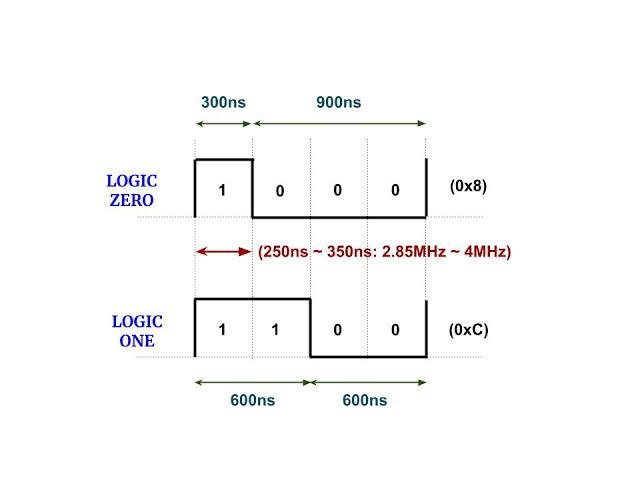
Thus set the SPI clock frequency to somewhere between 2.8hMHz and 4MHz, and use nibble (0x8) for logic zero, (0xc) for logic one. Then all should be good. Actually there are a few things to think about but let’s check the timing first.
The main clock used in the experiment was 12MHz. The frequency of the SPI clock was 3MHz (divided by 4). Value [0x88] was sent out via SPI bus and captured using DSO. In the picture below, the waveform shown above is the MOSI signal [0x88], and below is SCLK signal.
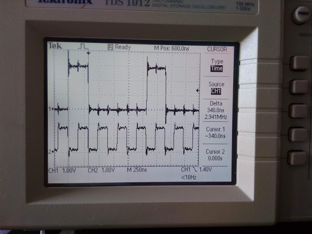
From the measurement, you can see that the width of the pulse is about 340nsec, 333nsec to be exact, and the width of zero period is 1000nsec, which fits the specification of logic zero. So the signal captured should be recognised as two consecutive zeros.
First thing to remember is that if you do not use DMA but use firmware code to send a stream of data to SPI bus one by one, then you will certainly see a gap between two consecutive data, which dose not recognized by the smart LED.
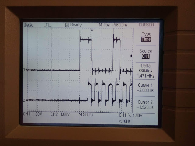
Second thing is when the SPI started to send its first byte, its data signal (MOSI) goes from zero to one sometime before its first clock appears if the first bit is one. It is shown in the following picture. MOSI waveform shown above leads the SPI clock below by 400nsec or so.
Thus although the same [0x88] data is sent as before, if this is the very first byte of the data stream, the pulse width of the first nibble is a bit thicker than the specification due to this fact. This will confuse the logic in the LED. To avoid this, your data stream should start with (0x0) nibble always. And actual data comes at the second nibble.
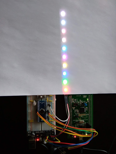
Following picture shows STM32L052 breakout board is driving a string of 10 SK6812 LEDs. The board on the right (ST32L0 discovery board) is used to program the board on the left.