AWS IoT FreeRTOS Sample

Amazon FreeRTOS sample code includes STM32L4 Discovery kit IoT node (B-L475E-IOT01A board), for compilation of which you need to install System Workbench for STM32, an Eclipse based IDE. However it can be avoided if you can build Makefile based environment with following steps.

(download source) Download the source code from Amazon and expand it into the directory of your choice, say AmazonFreeRTOS. It has three directories as explained in the directories.txt file.

(collect user folders) User files are in the two common directories under the demos.

Create a project directory, say aws_demos, create src subdirectory, and copy all the directories under two common directories into src.

(project root files) Populate the root folder of the project with following files:

  • Makefile
  • startup_stm32l475xx.s (startup code)
  • STM32L475VGTx_FLASH.ld (liker script)
  • jlinkcmd (JLink command script: optional)

Start up code can be found under

  demos/st/stm32l475_discovery/common/application_code/st_code

And linker script file can be found under

  demos/st/stm32l475_discovery/ac6

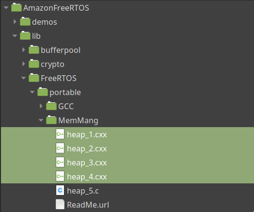
(remove unnecessary files) The source code comes with several files with the same definitions for memory handling, of which you are supposed to link only one file. The Makefile here collects source files automatically by the file extension. Thus you have to remove the unnecessary files from the directory or at least change the file extension. Otherwise you will have conflict definitions. In this case following files need to be removed. You need only heap_5.c.

(change Makefile) Finally, you may need change GCC_PATH variable to match your toolchain setting.

(source code)

WS2812(SK6812) Control with SPI and DMA

There are a couple of ways to control WS2812B and its clones. Among them, the method that uses SPI bus via DMA would be the easiest choice for the following reasons; Firstly SPI bus is ubiquitous. Secondly DMA minimizes the burden of the processor and handles timing with hardware. No code is involved in transferring data. Thus once proper SPI clock is chosen, operation is quite reliable as well. Only downside is that you have to dedicate one SPI port for the control of the LED, since you cannot share this line with any other SPI devices

The timing of SK6812 is shown below. There are slight variations in the actual timing between devices. But basically all use the same high/low ratio, namely 1:3 for logic zero and 2:2 for logic one.

Thus set the SPI clock frequency to somewhere between 2.8hMHz and 4MHz, and use nibble (0x8) for logic zero, (0xc) for logic one. Then all should be good. Actually there are a few things to think about but let’s check the timing first.

The main clock used in the experiment was 12MHz. The frequency of the SPI clock was 3MHz (divided by 4). Value [0x88] was sent out via SPI bus and captured using DSO. In the picture below, the waveform shown above is the MOSI signal [0x88], and below is SCLK signal.

From the measurement, you can see that the width of the pulse is about 340nsec, 333nsec to be exact, and the width of zero period is 1000nsec, which fits the specification of logic zero. So the signal captured should be recognised as two consecutive zeros.

First thing to remember is that if you do not use DMA but use firmware code to send a stream of data to SPI bus one by one, then you will certainly see a gap between two consecutive data, which dose not recognized by the smart LED.

Second thing is when the SPI started to send its first byte, its data signal (MOSI) goes from zero to one sometime before its first clock appears if the first bit is one. It is shown in the following picture. MOSI waveform shown above leads the SPI clock below by 400nsec or so.

Thus although the same [0x88] data is sent as before, if this is the very first byte of the data stream, the pulse width of the first nibble is a bit thicker than the specification due to this fact. This will confuse the logic in the LED. To avoid this, your data stream should start with (0x0) nibble always. And actual data comes at the second nibble.

Following picture shows STM32L052 breakout board is driving a string of 10 SK6812 LEDs. The board on the right (ST32L0 discovery board) is used to program the board on the left.

(source code)

UART Data Communication

In UART communication, TX process and RX process are usually handled differently. When transmitting data, you first construct a full packet of data. Then you send it rather relaxed manner. You can let the DMA handle the transfer, or you can use blocking call outside of any time critical function. Most of SDK provide such functions by default.

When receiving data however, you do not know the size or the validity of the packet beforehand. So you have to check each byte and verify it against the protocol as it arrives. Thus it is best to handle the RX task in an UART interrupt callback function instead of using functions provided by SDK.

In STM32Cube framework, you first activate UART RX interrupt using LL.

  412 /** Initialize SerialComm
  413  */
  414 void SerialComm_Init()
  415 {
  416     LL_USART_EnableIT_RXNE(huart1.Instance);
  417 }

Then write an interrupt handler for UART RX interrupt. In STM32Cube convention, a skeleton code for this interrupt handler is populated in stm32xxxx_it.c file.

  126 void USART1_IRQHandler(void)
  127 {
  128     if(LL_USART_IsActiveFlag_RXNE(USART1) && LL_USART_IsEnabledIT_RXNE(USART1))
  129     {
  130         SerialComm_RxRoutine();
  131     }
  132 }

In acutual RX routine, each incoming byte is checked by the packet decoder, SerialComm_Decoder and loaded into one of the two pingpong buffers whenever a valid packet is received.

  419 void SerialComm_RxRoutine()
  420 {
  421     pkt_status status;
  422 
  423     status = SerialComm_Decoder(LL_USART_ReceiveData8(huart1.Instance),
  424             UartIsrBuf);
  425 
  426     if(status == PKT_RECEIVED)
  427     {
  428         // switch ping pong buffer
  429         if(UartIsrBuf == UartRxBuf1)
  430         {
  431             UartIsrBuf = UartRxBuf2;
  432             UartRxBuf = UartRxBuf1;
  433         }
  434         else
  435         {
  436             UartIsrBuf = UartRxBuf1;
  437             UartRxBuf = UartRxBuf2;
  438         }
  439         // raise flag
  440         bPktReceived = true;
  441     }
  442 }

Then you need another task that checks the contents of this pingpong buffer and generates events when new packet is loaded.

  386 void UartRxTask()
  387 {
  388     int i;
  389     uint8_t event[EVT_QWIDTH];
  390 
  391     // packet received
  392     if(bPktReceived)
  393     {
  394         // event id
  395         event[0] = EVT_UART_RXPKT;
  396         // event data size
  397         event[1] = UartRxBuf[1];
  398 
  399         // copy the payload
  400         for(i = 0; i< UartRxBuf[1]; i++)
  401         {
  402             event[2+i] = UartRxBuf[2+i];
  403         }
  404     
  405         // register the event
  406         Evt_EnQueue(event);
  407         // clear the flag
  408         bPktReceived = 0;
  409     }
  410 }

This task runs as a software timer routine in regular interval, whose frequency should be higher than packet rate that the protocol defines.

  107     // start a timer routine: 10msec period, perpetual
  108     result = UsrTimer_Set(10, 0, UartRxTask);

This seemingly redundant UartRxTask is necessary to avoid race condition since EvtQueue is designed to be used by software timer callback for posting event. If Evt_EnQueue function is called from SerialComm_RxRoutine, a callback of the UART RX interrupt directly it can be disturbed by SysTick interrupt whose priority is higher.

Pushbutton Event Handler: Part 4

Pushbutton Handler

The handler routine is started by calling PushButton_Init function. This function registers PushButton_Routine at the end as a callback of the software timer.

   35 void PushButton_Init(uint8_t mask)
   36 {
   37     int i ;
   38 
   39     // clear data
   40     pp.old_state = pp.new_state = 0;
   41     pp.mask = mask;
   42     pp.mode = 0;
   43     pp.flag = false;
   44 
   45     // clear log
   46     for(i = 0; i < 8; i++)
   47     {
   48         PushButton_ClearLog(i);
   49     }
   50 
   51     // register pushbutton main routine
   52     UsrTimer_Set(PUSHBTN_TMR_PERIOD, 0, PushButton_Routine);
   53 }

The PushButton_Routine is then called at every 80msec and tracks the button state. If the button state is ON for at least three consecutive polling (80 x 3 = 240msec) then it declares CLICK by posting an event. These timing can be set to fit the bouncing characteristic of the mechanical switch.

   71 /// PushButton_Routine timer period in msec
   72 #define PUSHBTN_TMR_PERIOD      80
   73 /// Criteria for determination of short click and long click
   74 #define PUSHBTN_TO_SHORT        3       // 3 * PUSHBTN_TMR_PERIOD
   75 #define PUSHBTN_TO_LONG         10      // 10 * PUSHBTN_TMR_PERIOD
   76 #define PUSHBTN_TO_MAX          255     // maximum duration count

The PushButton_Routine, distinguishes single, double, triple click and long click (push and hold) and generates event accordingly, which in turn collected by the event handler in the main loop.

You can also change the mode from click detection to up/down detection, in which event is constantly generated when you hold the button down.

(source code)

Fixing B-L475E-IoT01A Board Reset Issue

There are at least two revisions of the B-L475E-IOT0A board. Earlier boards (version C) have rather critical bug in the hardware, so the STLink-V2 does not work. This is because the NRST net between STLink and the main MCU is missing in the version C board. For more information, check the manual. Unfortunately the manual didn’t describe how to fix it, although it is rather straightforward.

Grab a soldering tools and connect two points shown below.

On the schematic, these two points correspond to

and

USB MSD Device with SD Card

Build a low level driver for SD card, then the glue logic for FatFs and USB MSD is pretty much the same as Flash memory case posed before. In case of SD card, sector size is 512 in most of the cases. Thus the memory requirement is much relaxed. You can even allocate a file buffer bigger than the sector size.

FatFs site has a dedicated page for MMC/SDC, on which you can find fairly detailed explanation about how to interface MMC/SDC via SPI bus. Implementation should be straightforward until you encounter with cheap SD cards that do not behave very well.

In such cases, you either have to protect your code with redundancy or just stick with quality devices. If you choose SanDisk or Kingston brand, you will be safe. ADATA on the other hand, frequently generates timeout error at first try.

Most of the SD card sockets have a pin to detect the presence of the card. This pin is usually connected to GND pin or some other pin. You can use this to generate interrupt whenever a card is inserted or removed.

When inserted, run FATFS_LinkDriver() and call f_mount. When removed, you need to call FATFS_UnLinkDriver() to clear the disk state.

  596         // card is removed
  597         if(HAL_GPIO_ReadPin(SDC_EX_GPIO_Port, SDC_EX_Pin))
  598         {
  599             // reset SDCard state
  600             SDCard_SetStatus(SDCARD_NODISK);
  601             // decomission fatfs
  602             FATFS_UnLinkDriver(USERPath);
  603             DbgPrintf("\r\nSD card removed");
  604         }
  605         // card is inserted
  606         else
  607         {
  608             DbgPrintf("\r\nSD card inserted");
  609             // initialize fatfs
  610             retUSER = FATFS_LinkDriver(&USER_Driver, USERPath);
  611             // mount volume
  612             if((fr = f_mount(&USERFatFS, "/", 1)) == FR_OK)
  613             {
  614                 DbgPrintf("\r\nVolume mounted");
  615             }
  616             else
  617             {
  618                 DbgPrintf("\r\nFailed to mount volume:%d", fr);
  619             }
  620         }

This hot-plugging does not work however for USB MSD interface. You have to insert the card before you plug the device to the USB port of the host system. And do not remove the card during USB operation.

(source code)

Repurposing STLink of Nucleo64 Board

Most of the development kits from ST are equipped with on-board STLink-V2 debugger / programmers. However it is not very convenient to use in Linux environment.

Instead, Segger kindly provides a tool that allows you to reflash on-board STLink into JLink. Process takes only seconds. And you can enjoy most of the great features of JLink with no cost at least for STM32 devices. It keeps the UART port function, so you can use it as a serial monitor in addition to the JLink.

If you have a Nucleo-64 board handy, you can make a nice stand-alone JLink debugger by reflashing the on-board STLink and snap it off.

Note that the original pin headers are removed and some of them are replaced with right-angle type for the convenience. Two of the pins of ST-Link jumper are used to provide 3.3V power. And TX and RX pins of UART are soldered at the back not to interfere with the debug pins.

Note the small changes in the solder bridges SB3 through SB10. Basically this allows the 3V3 line to be connected to the first pin of the ST-Link jumper and GND line to the second through SB6. Both resistors are shunt (zero ohm).

Now you can use this breakout board to (1) power the target, (2) flash and debug via JLink and (3) have serial monitor connection all at the same time.

However beware the current limit of 150mA (actually lower than 150mA since the breakout board consumes some) of the LDO (LD3985M33R) used in the breakout board.

FatFs with FLASH Memory

STM32Cube framework provides similar interface for FatFS as USB MSC discussed before. Again the same argument applies to this case about the basic unit of read/write operation on a flash memory. In this case, the sector size and the cluster size of the FatFs should be equal to the sector size of FLASH memory, namely 4KB.

This can be set in the file ffconf.h, in which a lot of customization can be done by changing the definitions. In particular, following definitions should be set.

  204 #define _MIN_SS    4096  /* 512, 1024, 2048 or 4096 */
  205 #define _MAX_SS    4096  /* 512, 1024, 2048 or 4096 */

In the file user_diskio.c, USER_read and USER_write functions can be implemented as the same way as before. Here we assume that the count is always one for the simplicity. In fact this can be bigger than one if you call f_read() with the buffer size larger than the sector size (4096). However given the limited memory capacity of a mcu, that is not very realistic. And by similar token pdrv variable can be ignored.

    1 /**
    2   * @brief  Reads Sector(s) 
    3   * @param  pdrv: Physical drive number (0..)
    4   * @param  *buff: Data buffer to store read data
    5   * @param  sector: Sector address (LBA)
    6   * @param  count: Number of sectors to read (1..128)
    7   * @retval DRESULT: Operation result
    8   */
    9 DRESULT USER_read (
   10     BYTE pdrv,      /* Physical drive nmuber to identify the drive */
   11     BYTE *buff,     /* Data buffer to store read data */
   12     DWORD sector,   /* Sector address in LBA */
   13     UINT count      /* Number of sectors to read */
   14 )
   15 {
   16   /* USER CODE BEGIN READ */
   17     SFlash_ReadSector(sector, (uint8_t*)buff);
   18     return RES_OK;
   19   /* USER CODE END READ */
   20 }
   21 
   22 /**
   23   * @brief  Writes Sector(s)  
   24   * @param  pdrv: Physical drive number (0..)
   25   * @param  *buff: Data to be written
   26   * @param  sector: Sector address (LBA)
   27   * @param  count: Number of sectors to write (1..128)
   28   * @retval DRESULT: Operation result
   29   */
   30 #if _USE_WRITE == 1
   31 DRESULT USER_write (
   32     BYTE pdrv,          /* Physical drive nmuber to identify the drive */
   33     const BYTE *buff,   /* Data to be written */
   34     DWORD sector,       /* Sector address in LBA */
   35     UINT count          /* Number of sectors to write */
   36 )
   37 { 
   38   /* USER CODE BEGIN WRITE */
   39     SFlash_WriteSector(sector, (uint8_t*)buff);
   40     /* USER CODE HERE */
   41     return RES_OK;
   42   /* USER CODE END WRITE */
   43 }
   44 #endif /* _USE_WRITE == 1 */

If ioctl is to be used, implement corresponding parts in the USER_ioctl function.

   84 #if _USE_IOCTL == 1
   85 DRESULT USER_ioctl (
   86     BYTE pdrv,      /* Physical drive nmuber (0..) */
   87     BYTE cmd,       /* Control code */
   88     void *buff      /* Buffer to send/receive control data */
   89 )
   90 {
   91   /* USER CODE BEGIN IOCTL */
   92     DRESULT res = RES_ERROR;
   93 
   94     switch (cmd)
   95     {
   96     case CTRL_SYNC :
   97         res = RES_OK;
   98         break;
   99 
  100     case GET_SECTOR_COUNT :
  101         *(DWORD*)buff = SFLASH_NUM_SECTORS;
  102         res = RES_OK;
  103         break;
  104 
  105     case GET_SECTOR_SIZE :
  106         *(WORD*)buff = SFLASH_SECTOR_SIZE;
  107         res = RES_OK;
  108         break;
  109 
  110     case GET_BLOCK_SIZE :
  111         *(DWORD*)buff = SFLASH_SECTOR_SIZE;
  112         res = RES_OK;
  113         break;
  114 
  115     default:
  116         res = RES_PARERR;
  117         break;
  118     }
  119 
  120     return res;
  121   /* USER CODE END IOCTL */
  122 }
  123 #endif /* _USE_IOCTL == 1 */

FatFs allows users to not only read and write files but also to create a file system on a raw media. Unfortunately in this particular case, the capacity of the media is too small (1MB) for the FatFs to compute correct parameters. Thus its f_mkfs function failed. However, as shown before the file system can be created by the host system if it is connected to the host a s USB MSC device.

(source code)

USB MSC Device with FLASH Memory

USB Mass Storage Class implements bulk-only-transfer (BOT) with SCSI protocol. USB packets from the host eventually converted into SCSI transport commands by the middleware, in which data is exchanged (read / write) with the unit of logical block, typically 512 bytes.

This SCSI commands works well with SD card system where a dedicated controller does the job of managing the actual memory elements. If you want to use a FLASH chip as a memory unit instead, you need to handle read / write operation directly.

Fortunately, most of flash memory support 4KB block erase. This makes the 4096 bytes as a natural choice for the size of the logical block. In STM32Cube framework this is defined in the file usbd_storage_if.c

   94 #define STORAGE_LUN_NBR                  1
   95 #define STORAGE_BLK_NBR                  0x10000
   96 #define STORAGE_BLK_SIZ                  0x200

During initial enumeration, this information is registered to the host. The middleware maintains one logical block size of buffer and handles USB transaction whose each payload is only 64 bytes. It then calls SCSI requests to store / retrieve data to / from physical memory device in this case a FLASH memory when the buffer is filled. Thus the buffer size should be increased by the same amount in the file usbd_conf.h

  108 #define MSC_MEDIA_PACKET     4096

Now, remaing task is to simply convert SCSI block read/write commands into FLASH memory sector read/write operations.

    1 /**
    2   * @brief  .
    3   * @param  lun: .
    4   * @retval USBD_OK if all operations are OK else USBD_FAIL
    5   */
    6 int8_t STORAGE_Read_FS(uint8_t lun, uint8_t *buf, uint32_t blk_addr, uint16_t blk_len)
    7 {
    8   /* USER CODE BEGIN 6 */
    9     SFlash_ReadSector(blk_addr, buf);
   10     return (USBD_OK);
   11   /* USER CODE END 6 */
   12 }
   13 
   14 /**
   15   * @brief  .
   16   * @param  lun: .
   17   * @retval USBD_OK if all operations are OK else USBD_FAIL
   18   */
   19 int8_t STORAGE_Write_FS(uint8_t lun, uint8_t *buf, uint32_t blk_addr, uint16_t blk_len)
   20 {
   21   /* USER CODE BEGIN 7 */
   22     SFlash_WriteSector(blk_addr, buf);
   23     return (USBD_OK);
   24   /* USER CODE END 7 */
   25 }

Here the logical unit number(lun) is always zero. This is because there is only one LUN is defined. And the number of logical blocks (blk_len) is always one. This is because the internal buffer size is equal to the size of local block. See MSC_MEDIA_PACKET definition above.

When it is first plugged in, it appears as a raw disk with no FAT. So no logical drive will appear as if unformatted drive. It is necessary to create a FAT using fdisk. To minimize the overhead space, choose FAT16 <32M option in the fdisk (or cfdisk) utility.

Then format the drive

sudo mkfs.vfat -F 16 /dev/sdb1

At this point the host system may recognize the device as a formatted disk drive. Otherwise plug it out and in again. In the picture below, Nucleo32-L432KC (at the center) and Adesto AT25SF081 (bottom left) are used in this project. 

(source code)

STM32L052 Touch Sensor

Some of STM32 MCUs are equipped with TSC (Touch Sensing Controller), whose hardware performance is comparable to ASIC solutions. It is a self-sufficient module supporting multi-touch with decent SNR. And you can lower its power consumption down to few tens of micro amps.

Setting up the TSC requires to select one port for sampling for each group. One group consists of one sampling channel, where a sampling capacitor is connected, with one or more measurement channel, where a sensor pad is connected.

In each group, charge transferred from a measurement channel to the sampling channel automatically without firmware intervention. This is done independently from other groups. Thus channels belongs to each group are measured at the same time. In the same group, however measurement should be done sequentially among channels.

Following picture shows the test setup. A PCB touch panel on the right is connected to the STM32L052 breakout board on the left.

The MCU is programmed to measure the touch sensor value at every 100 msec. It transfers the measurement to a PC via UART connection. On the PC side, a python utility is prepared to collect data.

The python script also shows real-time plots as well as simple statistical data. From this data, you can easily check certain characteristics of the touch pad such as SNR, long-term drift, as well as the effect of the front cover structure on the sensitivity of the sensor.

It varies depending on the situation, minimum SNR of around 4 is considered to be necessary for the reliable operation. If the SNR is smaller than 3, additional post processing is required. If the noise is random, simple averaging can enhance the SNR effectively. Otherwise things get complicated. You may need to activate the spread spectrum (clock jittering) feature of the controller to make the noise spread out.

(source code)